- 您现在的位置:买卖IC网 > Sheet目录3753 > ATMEGA169P-16MCHR (Atmel)MCU AVR 16KB FLASH 16MHZ 64-VQFN
2005 Microchip Technology Inc.
Preliminary
DS41265A-page 157
PIC16F946
12.4
Effects of Reset
A device Reset forces all registers to their Reset state.
Thus, the A/D module is turned off and any pending
conversion
is
aborted.
The
ADRESH:ADRESL
registers are unchanged.
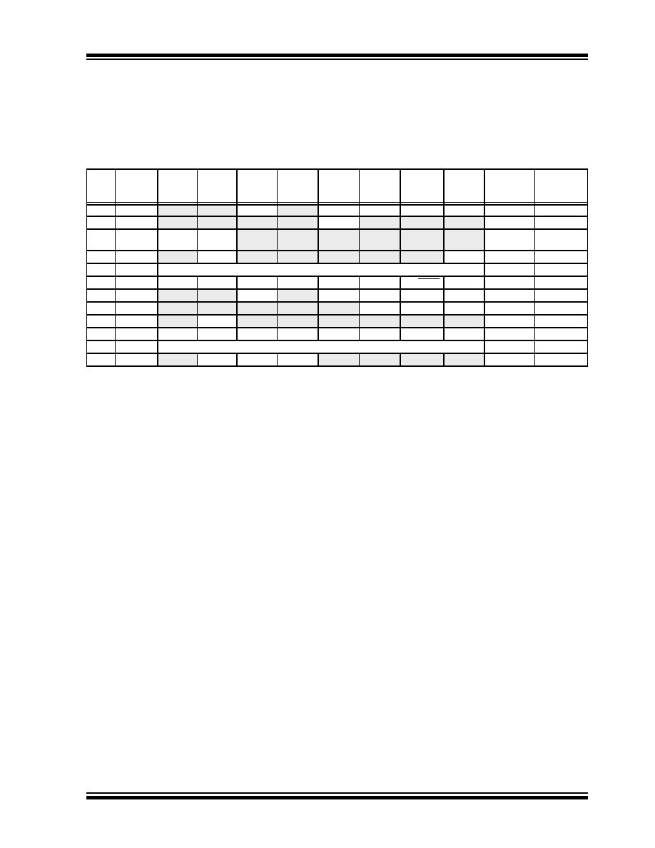
TABLE 12-2:
SUMMARY OF A/D REGISTERS
Addr
Name
Bit 7
Bit 6
Bit 5
Bit 4
Bit 3
Bit 2
Bit 1
Bit 0
Value on:
POR, BOR
Value on
all other
Resets
05h
PORTA
RA7
RA6
RA5
RA4
RA3
RA2
RA1
RA0
xxxx xxxx
uuuu uuuu
09h
PORTE
RE7
RE6
RE5
RE4
RE3
RE2
RE1
RE0
xxxx xxxx
uuuu uuuu
0Bh/
8Bh
INTCON
GIE
PEIE
T0IE
INTE
RBIE
T0IF
INTF
RBIF
0000 000x
0Ch
PIR1
EEIF
ADIF
RCIF
TXIF
SSPIF
CCP1IF
TMR2IF
TMR1IF
0000 0000
1Eh
ADRESH
Most Significant 8 bits of the left justified A/D result or 2 bits of the right justified result
xxxx xxxx
uuuu uuuu
1Fh
ADCON0
ADFM
VCFG1
VCFG0
CHS2
CHS1
CHS0
GO/DONE
ADON
0000 0000
85h
TRISA
TRISA7
TRISA6
TRISA5
TRISA4
TRISA3
TRISA2
TRISA1
TRISA0
1111 1111
89h
TRISE
TRISE7
TRISE6
TRISE5
TRISE4
TRISE3
TRISE2
TRISE1
TRISE0
1111 1111
8Ch
PIE1
EEIE
ADIE
RCIE
TXIE
SSPIE
CCP1IE
TMR2IE
TMR1IE
0000 0000
91h
ANSEL
ANS7
ANS6
ANS5
ANS4
ANS3
ANS2
ANS1
ANS0
1111 1111
9Eh
ADRESL
Least Significant 2 bits of the left justified A/D result or 8 bits of the right justified result
xxxx xxxx
uuuu uuuu
9Fh
ADCON1
—
ADCS2
ADCS1
ADCS0
—
-000 ----
Legend:
x
= unknown, u = unchanged, – = unimplemented read as ‘0’. Shaded cells are not used for A/D module.
发布紧急采购,3分钟左右您将得到回复。
相关PDF资料
2-1546217-0
TERM BLK RCPT 20POS SIDE 5.08MM
1-1546217-9
TERM BLK RCPT 19POS SIDE 5.08MM
1-1546217-8
TERM BLK RCPT 18POS SIDE 5.08MM
1-1546217-7
TERM BLK RCPT 17POS SIDE 5.08MM
1-1546217-6
TERM BLK RCPT 16POS SIDE 5.08MM
1-1546217-5
TERM BLK RCPT 15POS SIDE 5.08MM
1-1546217-4
TERM BLK RCPT 14POS SIDE 5.08MM
1-1546217-3
TERM BLK RCPT 13POS SIDE 5.08MM
相关代理商/技术参数
ATMEGA169P-16MCU
功能描述:8位微控制器 -MCU AVR 16KB, 512B EE 16MHz 1KB SRAM, 5V
RoHS:否 制造商:Silicon Labs 核心:8051 处理器系列:C8051F39x 数据总线宽度:8 bit 最大时钟频率:50 MHz 程序存储器大小:16 KB 数据 RAM 大小:1 KB 片上 ADC:Yes 工作电源电压:1.8 V to 3.6 V 工作温度范围:- 40 C to + 105 C 封装 / 箱体:QFN-20 安装风格:SMD/SMT
ATMEGA169P-16MU
功能描述:8位微控制器 -MCU AVR 16K FLASH 512B EE 1K SRAM LCD ADC RoHS:否 制造商:Silicon Labs 核心:8051 处理器系列:C8051F39x 数据总线宽度:8 bit 最大时钟频率:50 MHz 程序存储器大小:16 KB 数据 RAM 大小:1 KB 片上 ADC:Yes 工作电源电压:1.8 V to 3.6 V 工作温度范围:- 40 C to + 105 C 封装 / 箱体:QFN-20 安装风格:SMD/SMT
ATMEGA169P-16MU SL383
制造商:Atmel Corporation 功能描述:MCU 8BIT ATMEGA RISC 16KB FLASH 3.3V/5V 64PIN MLF - Tape and Reel
ATMEGA169P-16MUR
功能描述:8位微控制器 -MCU AVR LCD 16KB FLSH EE 512B 1KB SRAM-16MHZ RoHS:否 制造商:Silicon Labs 核心:8051 处理器系列:C8051F39x 数据总线宽度:8 bit 最大时钟频率:50 MHz 程序存储器大小:16 KB 数据 RAM 大小:1 KB 片上 ADC:Yes 工作电源电压:1.8 V to 3.6 V 工作温度范围:- 40 C to + 105 C 封装 / 箱体:QFN-20 安装风格:SMD/SMT
ATMEGA169P-8AU
制造商:ATMEL 制造商全称:ATMEL Corporation 功能描述:Microcontroller with 16K Bytes In-System Programmable Flash
ATMEGA169P-8MU
制造商:ATMEL 制造商全称:ATMEL Corporation 功能描述:Microcontroller with 16K Bytes In-System Programmable Flash
ATMEGA169PA
制造商:ATMEL 制造商全称:ATMEL Corporation 功能描述:8-bit Microcontroller with 16K Bytes In-System Programmable Flash
ATMEGA169PA_1
制造商:ATMEL 制造商全称:ATMEL Corporation 功能描述:High Endurance Non-volatile Memory segments